 The Handelot Times
TSMC, the chipset maker, will hire more than 8,000 engineers
TSMC plans to add 8000 jobs for a new R&D center which is expected to be completed by the end of 2022. It will be geared towards research and development for 3nm and beyond process technology.
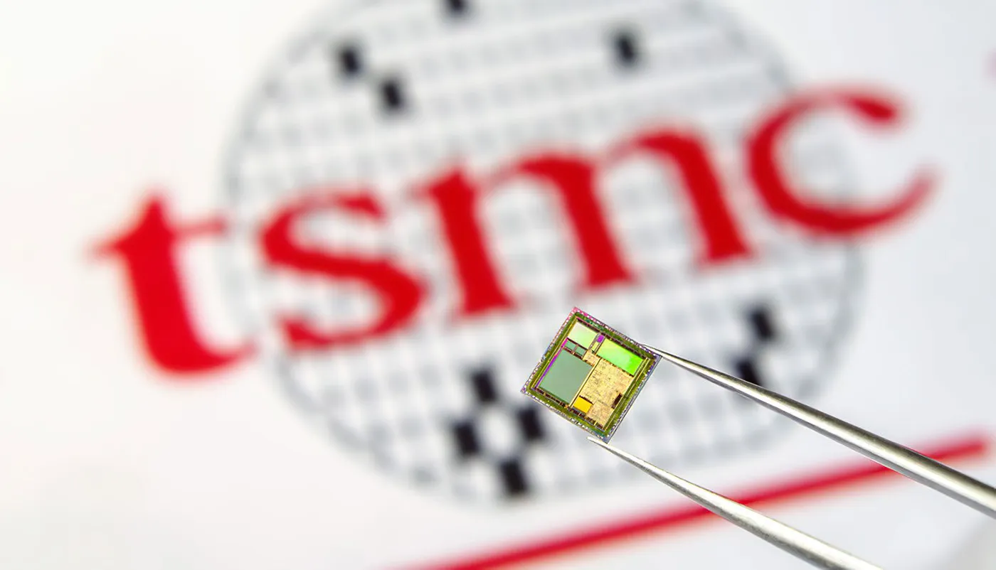
TSMC plans to add 8000 jobs for a new R&D center which is expected to be completed by the end of 2022. It will be geared towards research and development for 3nm and beyond process technology. That was announced by Mark Liu, TSMC CEO in the last Annual conference, who said they will hire an additional 8,000 employees for the center. The new R&D center will be located in northern Taiwan. Construction is scheduled to begin early next year and is expected to be completed by the end of the year. According to Taiwan News, an employee said he would dedicate himself to the development of 3nm.
We know that TSMC already works on the 5nm nodes for the next generation of chips, but the 3nm nodes are in the plans. At the moment, we do not know if nodes even smaller than 3 nm will arrive or if any other alternative to reducing nodes will be found to improve the performance of the processors and their energy consumption.
TSMC ended 2018 with some 49,000 employees, so adding 8,000 would mean a strong increase in its R&D capacity. In its most recent third quarter, TSMC spent $ 769 million on research and development, 10% more than a year ago. They recently started the construction of a factory in which to develop the 3nm chips.
TSMC recently started construction of a $ 19.5 billion manufacturing facility that will produce 3-nanometer chips starting in 2023. Technologically speaking, the Taiwanese foundry is “working with customers and progress in technology development is going well. . Our N3 process will be different from 5 nanometers with an improvement in PPA (power, performance and area, i.e. consumption, performance and area) similar to that between N7 and N5. We expect our 3 nanometer technology to be the most advanced for both PPAs and transistors when it is introduced. “ Overall, TSMC has invested $ 50 billion in fine-tuning the manufacturing processes that are used by its customers today. Recall that in recent weeks the company has indicated its intention to invest an additional 4 billion dollars in machinery to expand the production of 7 and 5 nanometer chips. Of these 1.5 billion will go to 7 nanometers, while 2.5 billion to 5 nanometers. TSMC will therefore bring the ‘capex’ in 2019 from 11 to 14/15 billion dollars.
More in Markets
 Markets
Salt instead of scarcity: how CATL’s sodium battery launch redraws the map of the energy transition
 Markets
Quick hits: TikTok saved, sort of, and SpaceX swallows xAI in the largest merger in history
 Markets
Big Tech’s power shift: who owns AI, who owns the future
 Markets
The $3 trillion IPO summer: SpaceX, OpenAI and Anthropic go public